|
|
|
| SPIE Advanced Lithography 2013 |
|
|
|
|
SPIE Advanced Lithography 2013 |
Closed
|
| world's premier semiconductor lithography conference and exhibition |
| Dates:
Sunday, February 24, 2013 - Thursday, February 28, 2013
|
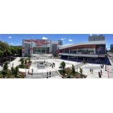
| Venue: San Jose Convention Center,
San Francisco,
United States |
|
|
SPIE Advanced Lithography is the world's premier semiconductor lithography conference and exhibition. The 2013 event is scheduled for 24-28 February, in San Jose, California.
Many of the industry's top semiconductor suppliers, integrators, and manufacturers take part in the annual SPIE Advanced Lithography exhibition. For 36 years SPIE Advanced Lithography has been the premier international event that drives the future of lithography research and applications.
Featured technologies at Advanced Lithography include:
• Etch Technology for nanopatterning
• Lithography: immersion, double patterning, e-beam, EUV, optical/laser, RET
• Metrology, inspection, OPC, and process control
• Design and manufacturing software
• Materials and chemicals
• Imaging equipment
• Lasers
• Resist materials and processing
• Nano-imprint
• IC and chip fabrication
• Nanoscale imaging
|
Website: http://spie.org/
|
|
|
|
|