|
|
|
| SPIE Advanced Lithography + Patterning 2027 |
|
|
|
|
SPIE Advanced Lithography + Patterning 2027 |
207 days left
|
| World's premier semiconductor lithography conference and exhibition |
| Dates:
Sunday, February 21, 2027 - Thursday, February 25, 2027
|
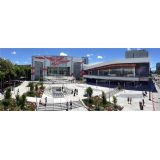
| Venue: San Jose McEnery Convention Center,
San Jose CA,
United States |
|
|
The SPIE Advanced Lithography + Patterning Symposium has been the showcase of the latest advances in lithography and patterning technology for over four decades. The technology landscape keeps on evolving to incubate more sophisticated and diversified information and computing technologies. The semiconductor technology sector, now in the More-than-Moore era, is facing more challenges that require holistic patterning solutions that involve a higher level of interactions among process technologies, devices, and system design sectors. The symposium will cover the full spectrum of the advances and challenges in state-of-the art lithography and integrated patterning technology through several topical conferences. Advances in areas of nano- and micro-patterning for semiconductor IC device applications will be presented in sessions covering optical lithography, extreme-UV (EUV) lithography, computational patterning, metrology/inspection, patterning materials, etch/deposition technology, and System-Design-Technology co-optimization. As novel patterning and non-IC lithography technologies, such as heterogenous wafer packaging, IoT devices including micro-machines and microsensors, AR/VR devices, FP Displays, have become more widely explored, related topics in these areas are also addressed.
|
Website: https://spie.org/x10942.xml
|
|
|
|
|